inquiry about designing a pcb with cavity
Fantomas , 07-01-2021, 05:50 AM
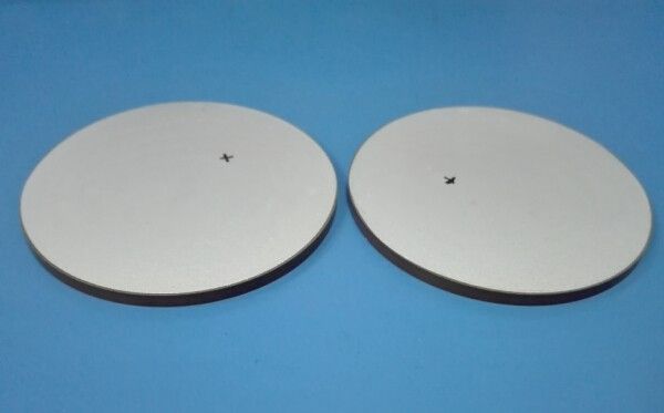
 I have a question about the possibility to add a cavity of 0.7mm on the PCB bellow, in order to insert a piezo ceramic disc, I would like to do the cavity in the center of this circular PCB,
the circle is marked with white, how can this be done on Altium designer? the pcb will have only one layer.
Thanks for your answer.
robertferanec , 07-02-2021, 05:21 AM
Do you mean like removing 0.7mm from the area in side of the white circle?
I am not sure if that can be done directly, but maybe it could be done through a "second PCB stackup" and using regions (?). Have a look at some videos about FLEX in Altium - that could give you and idea what I mean e.g. https://www.youtube.com/watch?v=9kMbNKiDJLo
But that would be basically only to show it in 3D. For manufacturing you can probably just tell that information in manufacturing notes.
Comments:
Fantomas, 07-05-2021, 12:42 AM
YES, it is about removing 0.7mm from the circle area.i got the same response from an manufacturer, they've told me that this type of direct pcb design is not supported.Thanks for your answer Robert.
WhoKnewKnows , 07-05-2021, 07:49 AM
Hello, I get email promotion from a fab shop that advertises pcb manufacturing with cavities. I'll try to find a link
Comments:
Fantomas, 07-05-2021, 07:51 AM
hello,thanks, but first i'd like to learn how to make it on Altium, if you can help!
WhoKnewKnows , 07-05-2021, 07:58 AM
Unable to find the original link, but a quick Goggle turns up a lot of hits, so appears to be a popular process/feature. No doubt you can find a fab shop that supports making cavities in PCBs
WhoKnewKnows , 07-05-2021, 08:00 PM
I think your best bet is using Altium 21. I'm not equipped to teach you, but Altium's YouTube channel has a playlist of videos "what's new in Altium 21" or some such. A video in that playlist describes lots of capabilities with controlling the stackup using regions as Robert suggested originally. Good luck 🤞
qdrives , 07-06-2021, 04:17 PM
Are you talking about depth routing?
In Altium I would just mark the area in a drawing and state that depth routing is required in that area (and how much)

In Altium I would just mark the area in a drawing and state that depth routing is required in that area (and how much)
Use our interactive Discord forum to reply or ask new questions.