Polygon Pour does not connect some ground pins
nick38 , 01-14-2023, 09:09 AM
Hi,
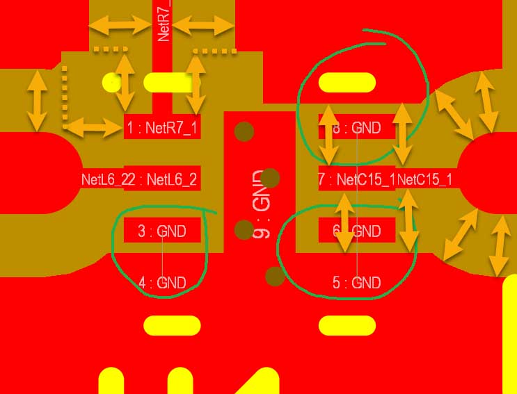
I'm using the Polygon Pour option to create a ground plane on the top layer, but I noticed that some pads are not being connected and after spending several hours on this I'm not able to find why.
Any idea what might be causing this and how to solve it?
I suspect some kind of clearance rule issue. I've configured a clearance of 0.6mm between copper-track and also copper and SMD pad. Because I need 0.6mm clearance for the transmission lines. Maybe there is a way to ignore this clearance for the IC pads.
I'll attach some pictures.
Thanks!


WhoKnewKnows , 01-14-2023, 10:36 AM
Interesting. In the first image it would appear polygon filling is obstructed by a clearance rule. I marked up that image and attached. Uncertain about the middle image, but I imaging that 3-pad footprint has its left and right pads, that require some clearance, so close together that the polygon settings won't allow a narrow enough "neck" to extend to that center ground pad. Perhaps fiddle with the Polygon settings. Things like minimum island, maximum neck and such may help your polygon not be so bashful?
Polygon fills are often temperamental like this. You might take advantage of the way Altium allows overlapping copper objects to form a single coper layer definition. EG tracks overlap pads and so on. You might place a fill on the same layer to "bridge" between the polygon and a same-net object you want the polygon to stop being bashful about connecting. I don't recommend this as a solution, but by placing a track or fill, the connection may likely be forced, the perceived needed clearance violated, this may cause Altium to reveal what rule if any is offended.
See also in rules: Polygon connection style.
Perhaps also check individual footprint pads for their connection setting.
Good luck! 🤞
nick38 , 01-14-2023, 12:06 PM
I changed the pour option to "Pour Over All Same Net Objects" and it looks better, but I had to add a new clearance rule with a custom query that has "HasFootPrint('QFN16') so that it doesnt trigger rule violations on the pads of the IC. Some of the pour around the pads look funny because of the 0.6mm clearance that I need. Is there anyway to solve this? maybe there is a way to define an area around the IC so that the 0.6mm clearance rule does not apply?

WhoKnewKnows , 01-14-2023, 12:14 PM
I recall @robertferanec has a video about changing how rules work within a footprint. In it, he demonstrates how he can get a trace to go between two pads in a footprint without violation, but the normal rules take over outside of the footprint.
Alternatively, you could create a room that includes just a component or footprint and then use that for altering how rules work in that area of the PCB.
Alternatively, you could create a room that includes just a component or footprint and then use that for altering how rules work in that area of the PCB.
robertferanec , 01-19-2023, 11:34 PM
- double check clearance rule
- double check your polygon properties (e.g. Remove necks less than ...)
- double check pad / polygon thermal relief connection style (e.g. direct ?)
- double check pour settings e.g. "Pour Over All Same Net Objects"?
You can also simply draw a track there to connect it with the polygon - that is what I would probably do here (I would maybe draw a polygon pour cut out in the chip area and draw tracks manually to connect pins with polygon the way I would like to have them).
Use our interactive Discord forum to reply or ask new questions.