Silk to Silk & Silk to Solder Mask errors
nicolas.logioia , 06-27-2017, 03:44 PM
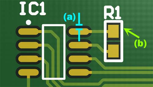
Hi guys! During Switching Power Supply course I found a problem with two errors in particular that I can't avoid!. It seems like Altium doesn't allow to overlap "text" (of the component, hidden for a more comfortable design) with a via or a bottom/top overlay layer (Silk to Silk error Clearance constraint). I believe this is not important as Robert did not have bottom overlay visible during design. Also, I get another error when overlaping text with pads of any component (Silk to Solder Mask error). What'silk? Sorry for these new starter questions; I'll let the pictures describe what's going on. THANKS A LOT!


mairomaster , 06-28-2017, 01:38 AM
Silkscreen is the term used for the visual/drawing information on the board. Usually it's white colour:

You don't want it to overlap pads for example - the pads need to be clean for good solderability. Also normally you would prefer to not overlap silkscreen object - for example 2 pieces of text. That's normally not critical but it's ugly in the very least.
You don't want it to overlap pads for example - the pads need to be clean for good solderability. Also normally you would prefer to not overlap silkscreen object - for example 2 pieces of text. That's normally not critical but it's ugly in the very least.
nicolas.logioia , 06-28-2017, 09:10 AM
Thanks! I'll make smaller text and re-organize things 
robertferanec , 06-28-2017, 11:54 PM
Yeah, you do not want to draw through pads. Some PCB manufacturer will remove the white color from pads, but not all of them. And if they do not remove it, you can imagine how difficult it may be to solder a component to that pads (you will probably need to remove the white color from the pads before you start soldering and it may not be easy - especially in mass production).
Use our interactive Discord forum to reply or ask new questions.