0.5mm Pitch eMMC Routing Issues
ibocakir06 , 01-30-2021, 11:21 AM
Hi all, I have a question about routing 0.5m Pitch BGA Fanout.
I have MTFC seires eMMC in my design. I want to make a fanout but the numbers are getting and getting smaller.
Issue 1:
Pitch: 0.5mm -> Ball Diameter: 0.25mm
In my design, minumun drill size is 0.2mm.
I dont want to decrease this number because of only one IC. Although if I use 0.15mm drill size, 0.3mm pad size via, the clearence is 2.998mil(Capture.png).
However my min. clearance is 4 mil.
Issue 2:
I googled the problem, NXP has an article about this: https://www.nxp.com/docs/en/applicat...te/AN10778.pdf
Issue 3:
I found another document about eMMC routing. Octavo says that, you can route through NC pads.
What dou you about Octavo's solution? Is it OK?
I need your opinion. Thanks in advance.
I have MTFC seires eMMC in my design. I want to make a fanout but the numbers are getting and getting smaller.
Issue 1:
Pitch: 0.5mm -> Ball Diameter: 0.25mm
In my design, minumun drill size is 0.2mm.
I dont want to decrease this number because of only one IC. Although if I use 0.15mm drill size, 0.3mm pad size via, the clearence is 2.998mil(Capture.png).
However my min. clearance is 4 mil.
Issue 2:
I googled the problem, NXP has an article about this: https://www.nxp.com/docs/en/applicat...te/AN10778.pdf
4.3 Recommended 0.5 mm pitch BGA via fan-out pattern
The pattern of centering the through-via within the four adjacent BGA land pads can not be used with 0.5 mm pitch BGA’s. This is due to the smallest through-via pad being too large to fit in the space available between the land pads. With a single trace routed between adjacent BGA land pads, the two outer rows of balls can be routed without a fan-out via. The two inner rows of balls must be routed to vias in the center area of the BGA and escape routed on other layers. An example fan-out of the LFBGA320 package is shown in Fig 6. See Table 5 for the layout tool design rules for 0.5 mm pitch BGA via fan-out.
The pattern of centering the through-via within the four adjacent BGA land pads can not be used with 0.5 mm pitch BGA’s. This is due to the smallest through-via pad being too large to fit in the space available between the land pads. With a single trace routed between adjacent BGA land pads, the two outer rows of balls can be routed without a fan-out via. The two inner rows of balls must be routed to vias in the center area of the BGA and escape routed on other layers. An example fan-out of the LFBGA320 package is shown in Fig 6. See Table 5 for the layout tool design rules for 0.5 mm pitch BGA via fan-out.
I found another document about eMMC routing. Octavo says that, you can route through NC pads.

What dou you about Octavo's solution? Is it OK?
I need your opinion. Thanks in advance.

robertferanec , 02-01-2021, 03:37 AM
I would have a look how they did it in reference design.
They may use VIA in pad to fanout, they may use super small VIAs, or as suggested, some footprints have space left for VIAs between pin rows under BGA, so you can use them.
PS: I do not like to use these super small BGAs, but I know, sometime not possible
PSS: Personally, I do not connect NC pins. I know some people do it.
ibocakir06 , 02-03-2021, 11:42 PM
Hi Robert, Thank you for your answer.
I have seen only 1 board which has eMMC and uploaded one snapshot of it.
- They may use VIA in pad to fanout : They didnt use via in pad.
- they may use super small VIAs : They didnt use small via. Dimensions: 0.2mm Drill, 0.45mm Pad
They routed tracks with 3mil track witdth and 4 mil clearance. I also dont want to do like this.
Do you mean, I can delete A7 pad route the track through it? Captured below.
Thank you.


robertferanec , 02-04-2021, 07:03 AM
The proper way to route it should be between pads. If you can't and there is no other option .... you can possibly get away with routing through a pad (I personally do not do that), but I would definitely not remove any pads (I am not sure how the melted ball would behave if there is no pad when the chip is soldered down)
ibocakir06 , 02-07-2021, 01:00 AM
OK Robert, I will not remove any pads, so all balls will be soldered down.
However, you did mentioned about Octavo's solution. Can it be the other option ? I want to route through NC pins. NC means, as you know, Not Connected Internally. So, if you route smt through NC pins, electrically effect will not be on eMMC chip.
However, you did mentioned about Octavo's solution. Can it be the other option ? I want to route through NC pins. NC means, as you know, Not Connected Internally. So, if you route smt through NC pins, electrically effect will not be on eMMC chip.
robertferanec , 02-08-2021, 01:18 AM
Theoretically connecting NC should not be a problem.
PS:
- it may be a little bit of stub on signal,
- also be sure that pin is not connected in future or in possible alternatives which you may use
PS:
- it may be a little bit of stub on signal,
- also be sure that pin is not connected in future or in possible alternatives which you may use
ibocakir06 , 02-08-2021, 01:49 AM
I will route through the NC pins, Robert.
Thank you for your great support
Thank you for your great support
ibocakir06 , 02-20-2021, 08:59 AM
Hi again,
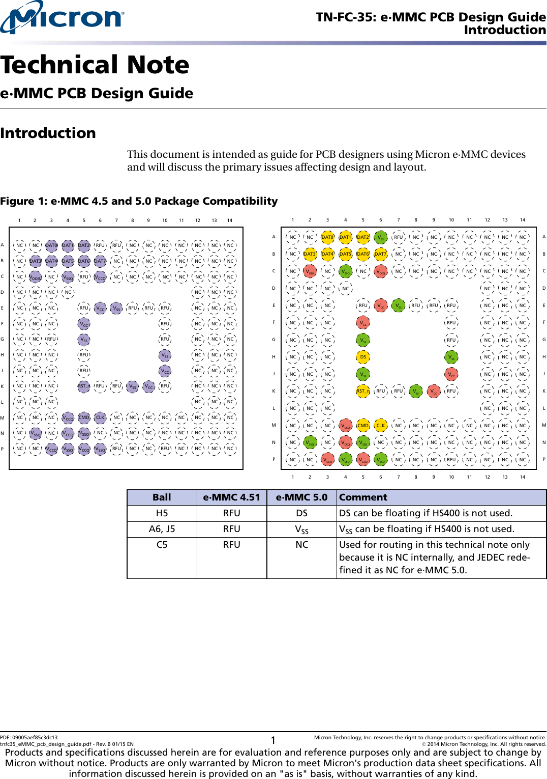
I found Micron's document which says you can route through NC pins 🤗
Please check it out !
I found Micron's document which says you can route through NC pins 🤗
Please check it out !
robertferanec , 02-22-2021, 02:06 AM
Thank you very much @ibocakir06 for sharing
ibocakir06 , 03-25-2021, 02:24 AM
Hi Dan, thank you for your attention.
I have designed the as I mention above tiwh routing throudh NC pins and have sent gerber files to my manufacturer. My board was 100x180mm 8 layer and min clearance is 4 mil, min track is 4 mil and min drill is 0.2mm. I have only TH vias and this is not a HDI board, no microvias.
I think if I design a IMX8 Mini or Nano (0.5mm pitch), I would definitely use smaller vias or clearances. Only for eMMC fanout I did not want to decrase my values to 3 mil. I doubted about working or not with this method until I have found the Micron's document I shared above.
I am waiting my board to be produced and I will also share here it is working or not.
Thanks.
İbrahim.
ibocakir06 , 03-25-2021, 02:35 AM
I am very glad with your comments, pls keep going
To comply with IPC standarts I use 0.2mm drill size and 0.45mm via pad. I see someone use 0.2mm drill and 0.4mm pad, but I dont use like this. So you have to descrase the values.
To comply with IPC standarts I use 0.2mm drill size and 0.45mm via pad. I see someone use 0.2mm drill and 0.4mm pad, but I dont use like this. So you have to descrase the values.
ibocakir06 , 03-25-2021, 03:07 AM
This is I am referring.

Use our interactive Discord forum to reply or ask new questions.