Reducing risks on one-unit-only prototypes woth expensive SocS
nachodizz990 , 05-28-2016, 01:04 PM
Hi all, i want to collect some ideas or some usefull tips when designing prototypes with very expensive hardware such as Altera Arria, Cyclone or Stratix SoC Famlies in order to avoid waste much money on prototyping phases where a fail can be a big problem.
I have fear to fail and I was thinking about a bga socket for example, so that if it works with the socket, further and without it, the integrity will be better or at least equal..., and if it fails i dont demage the SoC!, anyone has experience on prototyping with shuch systems?
I think that i will not find a bga socket for Altera uBGA 672 Wire Bonded packages

We´re designing a rangefinder embedded on a quadcopter with a lot of things and video transmit based on Altera soc family and i want to share the idea with you too !
This block is able(tested) to catch a very high speed pulse without needing to have a some ghz logic, by detecting changes in the register.
Perfect for a laser radar
4 Pll with the same multypling factor BUT whith different phase shift feeding an 8 bit register when 4 of then are negedge sensitive.
Thank you in advance!


mairomaster , 05-29-2016, 04:08 AM
I have done a couple of designs with Altera Arria/Cyclone, no problems whatsoever. I can advice you to thoroughly test you design first on a development board to be sure: first it is working the way you want it to and second you have all interfaces that you can potentially need wired. Having a good FPGA engineer helps a lot as well.
With the schematics/PCB check some reference designs from Altera, they have very good ones. The schematics should be relatively straight forward, however there are some small pitfalls which could be easily caught by reading the design guides. There is nothing hard with the PCBs - those FPGAs are big pitch devices so there shouldn't be any issues really if you are smart about it.
With the schematics/PCB check some reference designs from Altera, they have very good ones. The schematics should be relatively straight forward, however there are some small pitfalls which could be easily caught by reading the design guides. There is nothing hard with the PCBs - those FPGAs are big pitch devices so there shouldn't be any issues really if you are smart about it.
robertferanec , 05-29-2016, 09:54 AM
This is a big topic - and it is the main topic of Advanced Hardware Design course.
When I design boards, I am also very careful. I pay everything from my own money. When building a prototype costs 10 000 USD I need to be quite sure, that the first prototype will be working oki (not saying that I also pay for months of development).
I covered some topics in my blog:
- x86 Motherboard Development Process – Step by Step
- 8 Steps Schematic Checking Procedure
- Checking your PCB from a Mechanical point of view
- 10 Tips for Better Schematic Checking – Processor Boards
- ...
In your case. I have never used BGA socket, so I am not sure how reliable it is. And, I think the socket is very very expensive. If you follow reference designs you should not need the socket and you should just be fine. Be sure you check your schematic properly (our schematic & library checking often takes 2-3 weeks). In case something gets really wrong, you still will be able to rework the BGA chip.
If you are not sure, do a lot of testing with reference boards - and then just create your schematic based on it. If you have to design your own small circuits, make 1 layer PCBs and test everything. You would be surprised how simple circuits will not work as you would be expecting
nachodizz990 , 05-31-2016, 12:51 PM
PD2: Robert you have to deal with semiconductor manufacturers to sponsor your boards as terasic does (it costs more for me the soc than the complete dev board) but i cant place a dev board in my final product you know..
.
You are so popular i dont understand why they dont sponsor you ....
It´s so difficult?
.
You are so popular i dont understand why they dont sponsor you ....
It´s so difficult?
robertferanec , 06-01-2016, 12:35 AM
- Thank you
- If you would need to re-flow a BGA for 4 times, then there is something wrong with the design.
- none is sponsoring our projects. The managers of big companies see it different way All the projects and work we do is supported by people who buy our courses.
- If you would need to re-flow a BGA for 4 times, then there is something wrong with the design.
- none is sponsoring our projects. The managers of big companies see it different way
All the projects and work we do is supported by people who buy our courses.nachodizz990 , 06-02-2016, 01:11 PM
Yes i have to design with patience...
nachodizz990 , 06-02-2016, 01:21 PM
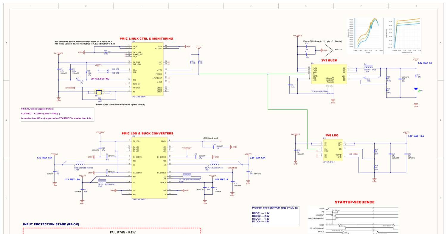
I modified the expensive power supply with a TI TPS65218 PCMIC, the other version was so powerfull but was about 28€ only the supply block, now is 4€ but i need too much power,
Perhaps adding 2A buck regulator separately for 3v3 but they are so exensive...
I will test the suply with some heat resistors and doing some tests to see their limits.
I think that the most cheaper is to try designing my own buck ...
I need some kind of soft start to chargue all capacitors that i will place.
Anybody tested the PowerSoc ICS? en6360qa soo expensive too but 8 Amps...
How is the performance of the OpenRex Pmic? , i choosed it because its a cheaper way, i will not use the i2c stuff, only the first time for burn the eeprom.Wold be fine to having a FLUKE thermal camera for observe the pcb heat stat...
By last
I´m not able to export a DIFF100 group to the layout editor, all it´s ok but it doesn´t appear as a class, only as a net on the PCB menu
What I´m doing Wrog?Thank you in advance

mairomaster , 06-02-2016, 05:04 PM
Can you provide some more information about what power rails you have, what ICs in total you need to power and how much current you need per rail.
For the boards I work on, for the FPGAs we use only Enpirion modules, including EN6360 I believe. The modules seem to be very good quality - no problems at all. You are right that they are a bit expensive though. Different PMICs are often designed for specific processors and often can't supply to much current per rail, which might be required for the core rails of the FPGA.
For the boards I work on, for the FPGAs we use only Enpirion modules, including EN6360 I believe. The modules seem to be very good quality - no problems at all. You are right that they are a bit expensive though. Different PMICs are often designed for specific processors and often can't supply to much current per rail, which might be required for the core rails of the FPGA.
nachodizz990 , 06-02-2016, 06:24 PM
Of course!
More or less: pci xpress, ADV7511, wolfson audio, ddr on fabric and hps 512 and 1Ghz respectively, cmos camera with d phy adapter for csi,usb, an amazing ADC12J4000,ethernet,probably a wilink,its a vitamined version of the nano soc for my needs.
Now the problem is the fabric, 2 core niosII f at 145 mhz with freertos,plus the dual cortex A8, at 925 mhz perhaps with Qnx,so probably the only problem is the fabric because the remaining its similar to the rex for example...
Perhaps the pmic will be enaoght with some capacitance, soft start and good heatsink... I Think that the empirion is too big for this case.The fabrik is 50k Le's and i use almost all for video compressing and maybe OpenCL
Another problem is that i will put expansion headers .... I want to use the pmic but... Maybe i need to make an simple 2 layer board with the pmic part and make it twist to test limits,another problem its Reliability, if this board was being sended to neptuno i will be more relaxed with empirion... Haha
robertferanec , 06-03-2016, 12:46 AM
As @mairomaster noted, PMICs are usually very specific. They have a lot of outputs, but the maximum currents are very limited. In past designs I have used ISL6236A (same is used on the iMX6 Rex module). If needed, this can easily deliver 10A.
nachodizz990 , 06-03-2016, 03:32 AM
I upgraded the supply, thanks for your recommendations.
Schematic here:
Schematic here:
nachodizz990 , 06-03-2016, 09:41 AM
Note the value of R14 R10 fail limit resistors is pending to set after testings compares with internal 800mv...
If someone sees any fail please comment it
If someone sees any fail please comment it

nachodizz990 , 07-10-2016, 10:48 PM
Almost Finished! Hope you like this !
Includes Cyclone V SoC and DAC38J84 full HDMI adv7513 etc...


mairomaster , 07-11-2016, 02:43 AM
It looks very good Are you confident with everything already?
Are you confident with everything already?robertferanec , 07-11-2016, 11:47 AM
What a beautiful board! Very nice.
robertferanec , 07-12-2016, 08:52 AM
Do not manufacture one unit - you want at least 3, ideally 5. You need more boards to compare the behaviour between them. Assembly process can bring tons of problems (bad soldering, bad component, misplaced component, wrong value component, ...) - and if you are unlucky and you build only one board with a faulty assembly it can take you ages to make it work.
If you do not use uVIAs, you should be able to get relatively "cheap" PCB (maybe up to 1000EUR?). Again, do not order 1 PCB, ask them to give you the maximum number of your PCBs which fits on the panel. Very often you can get 10 PCBs almost for the price of 3 (depends how big your PCB is and how big panel they use for manufacturing).
And, you really may want to buy new components - when you will be de-soldering parts, you may damage them and ... again ... you may spend ages by trying to figure out why something is not working.
I hope this helps.
nachodizz990 , 07-12-2016, 09:05 AM
Thank you robert the estimated costs are exactly what you said lab circuit spain plus 85 each pcb mi idea its to solder all components at home but the ddr and bga by predefined mini stencilcs on a rework house
Whats your opinion
Whats your opinion
robertferanec , 07-12-2016, 09:23 AM
You do not need stencil for BGA, use some flux and heat them up (we use hot air gun). You may need a little bit of practicing, but we have done that million times it works oki. However, for you it may be better go to a rework house if you have this possibility.
Note: This is not BGA, but it is a very similar procedure (for BGA you do not need to put tin on the pads, just the flux):http://www.fedevel.com/welldoneblog/...a-hot-air-gun/
Note: This is not BGA, but it is a very similar procedure (for BGA you do not need to put tin on the pads, just the flux):http://www.fedevel.com/welldoneblog/...a-hot-air-gun/
nachodizz990 , 07-12-2016, 10:16 AM
Oh! thank you again Robert you´re a monster engineer!
I prefer to go to with a Rework House because they have XRAY inspection... haha
But i will try to do it further to save costs.
I hope for find a pcb house that offers cheap 12 layers with pre-defined standard stackup and without uVias
Somewhere i read that if it´s a new pcb its not neccesary to use solder paste as you said! Only flux
But if it´s not a new pcb with an unconfirmed value of tin left on the pcb also if you removed all the tin i´ts recommended to use solder paste
nachodizz990 , 07-18-2016, 02:59 PM
I improved the component placing as you can see on the images and also routed almost all the board.
Due to the bad disposition of SoC ddr balls, i had to go with 12 layers but all trough hole vias.
I have 4 internal high speed signal layers but they are almost all empty excepting on the ddr3 area.I need one more power layer ...
I dont like this situation, my goal it´s to have a routing similar to the open rex ( it´s very nice) where all the layers are good filled
Would be perfect to be able to go with 10 layer
I´m planning to go for a bga 484 cyclone soc part instead od bga 672 reducing at the half the SoC price and may be the layer count ( i have to study all the bga io balls )
.
robertferanec , 07-19-2016, 06:12 PM
Fantastic progress
nachodizz990 , 07-19-2016, 06:31 PM
@robertferanec what can happen if i pullup the ethernet RGMII on the RNX9031 to the SOC 3V3 instead of pulling it up to the RNX9031 DVDDH that passes trough a ferrite bead?
Thank you in advance.
I´m trying to mathematically find the best RNX9031 decoupling scheme , i see your schematic, Terasic schematics and Texas Instruments Schematics and there are different.
I want to design my own board without copying to anyone.
The most easy to understand scheme it´s the Open Rex decoupling scheme ( 10 uf bulk, 100 nf cleaning after bulk and 10 nf at each pin) but i cant understand this approaches, i dont like to put decouplings without understand why these values are adecuate to my design
Comments:
robertferanec, 07-21-2016, 08:23 PM
What is RNX9031? Do you mean KSZ9031?
nachodizz990 , 07-20-2016, 07:55 AM
I´m evaluating if my power solution is the best choice for my design.I choosed this PMIC because it´s simple and cheap.
Actually i have a TPS65218 PMIC for 1.1V, 1.2V, 2.5V and 1.8V and two independent Bucks for 1.5V for DDR plus the termination LDO and another for 3.3 V for FPGA and IO
The TPS65218 PMIC haves 4 DCDC converters:
- DCDC 1, 2, 3 -> 1.8A max They generate 1.1 V - 1.2V for Processor System and 2.5 for Processor and FPGA
- DCDC 4 -> 1 A max It generates 1.8V for Ethernet and HDMI
In some development boards power blocks i see that 1.1V are rated for 3A and in others 6A ¿Are they crazy?
While running the altera Power Play Estimator (This Excel) i´m getting only 0.7 A required for 1.1V at full load
So i cant understand why the dev boards use 1.1V 3A DCDC SOLUTION
Just in case, i´m planing to change my power block replacing the TPS65218 PMIC by a TPS659037 solution (So much powerful and BGA )
Here the TPS659037 specs
One 0.7 to 1.65V at 6 A One 0.7 to 1.65 V at 4
One 0.7 to 3.3 V at 3 A
Two 0.7 to 3.3 V at 2 A
Two 0.7 to 3.3 V at 1 A
Seven General-Purpose LDO´s
Will my actual 1.1 V 1.8 A be suitable for A9 Dual Core At 924 MHZ ?
Thank you in advance !!
On the development board supplies schematics they have a total of 14 - 20 Ampsof total currents but the board is supplied with a 2A wall adapter
So i will desolder the inductors and measure currents with my Agilent U1273A at full loads, full- stressing the processor and FPGA
here´s nothing like real measurements !!
Here´s some strange
I think that a development board should be a reference design so overdimension of supplies are a WRONG WAY to do a reference board !!!
Maybe this is because they have the parts for free... I´m not !
Actually i have a TPS65218 PMIC for 1.1V, 1.2V, 2.5V and 1.8V and two independent Bucks for 1.5V for DDR plus the termination LDO and another for 3.3 V for FPGA and IO
The TPS65218 PMIC haves 4 DCDC converters:
- DCDC 1, 2, 3 -> 1.8A max They generate 1.1 V - 1.2V for Processor System and 2.5 for Processor and FPGA
- DCDC 4 -> 1 A max It generates 1.8V for Ethernet and HDMI
In some development boards power blocks i see that 1.1V are rated for 3A and in others 6A ¿Are they crazy?
While running the altera Power Play Estimator (This Excel) i´m getting only 0.7 A required for 1.1V at full load
So i cant understand why the dev boards use 1.1V 3A DCDC SOLUTION
Just in case, i´m planing to change my power block replacing the TPS65218 PMIC by a TPS659037 solution (So much powerful and BGA
)Here the TPS659037 specs
One 0.7 to 1.65V at 6 A One 0.7 to 1.65 V at 4
One 0.7 to 3.3 V at 3 A
Two 0.7 to 3.3 V at 2 A
Two 0.7 to 3.3 V at 1 A
Seven General-Purpose LDO´s
Will my actual 1.1 V 1.8 A be suitable for A9 Dual Core At 924 MHZ ?
Thank you in advance !!
On the development board supplies schematics they have a total of 14 - 20 Ampsof total currents but the board is supplied with a 2A wall adapter
So i will desolder the inductors and measure currents with my Agilent U1273A at full loads, full- stressing the processor and FPGA
here´s nothing like real measurements !!
Here´s some strange
I think that a development board should be a reference design so overdimension of supplies are a WRONG WAY to do a reference board !!!
Maybe this is because they have the parts for free... I´m not !

Comments:
robertferanec, 07-21-2016, 08:32 PM
Usually the high current regulators are used to cover current peaks. Also, sometimes the power is designed the way to get option to fit the most powerful pin to pin compatible chip or possibly next generation pin to pin compatible chips which you may not know about. I am always very careful about powers and if I am not sure, I use power supply with at least the same maximum current as they used in the reference design. If you underpower a rail, the board may be occasionally crashing (or behaving unstable or weird) and you may not be able to find out what is causing the problem. Debugging this kind of issue is extremely time consuming and it can be very frustrating.
robertferanec , 07-21-2016, 08:36 PM
@nachodizz990 I love your PMIC Schematic
Comments:
robertferanec, 07-21-2016, 08:42 PM
Yeah Why to discover the wheel
nachodizz990 , 07-22-2016, 05:00 PM
Sorry, i was mistaked ! The 1.8 Amp it´s really enought for the ARM A9 Dual core but i was forgetting that the FPGA also uses the same domain on shared mode ( is powered by the same 1.1V too) so i need at least 3A for 1.1V i will change PMIC!
I hope for someone can use my old schematic for doing a easy to use power solution, now i have to redesign the supply!
I´m using 5CSE without High Speed transceivers but the high end SoCs with high speed transceivers and a lot of logic elements need a peak current of 9A !!
Finally i go with two MAX17509ATJ a cheaper and most adecuate and powerfull solution removing the enpirion
@robertferanec yo was right !
mairomaster , 07-27-2016, 05:17 PM
Are you sure you will have enough space for length matching the RAM?
Comments:
nachodizz990, 07-27-2016, 05:31 PM
Guest thank you for your observation! but note that i have 4 internal layers for routing ddr due to de bad disposition of the DDR balls on this chip series. I tried once and i was succesfull now i´m starting from scratch again because i made a lot of changes but the next week i will start with DDR3 and i will be posting my progress, thank you for being interested
robertferanec , 07-30-2016, 06:32 PM
That is going to take some time to finish
robertferanec , 08-10-2016, 02:47 AM
Did you check if you can plug in a wide USB memory stick and RJ45 cable at the same time? Some USB dongles can be really wide: https://www.google.sk/search?q=usb+m...UIBigB&dpr=0.9
nachodizz990 , 08-10-2016, 05:28 AM
Thank you @robertferanec i will move the hub a little bit more to the front.
An important question i have it´s about the clocking, i´m generating ethernet, usb hub and phy (24mhz), and soc clocks from the Spread spectrum Clock Synthesizer (U9) and a 10 ppm oscillator. The usb chips are far away and i will route from synthesizer the 24 mhz clock to both chips in t branch, do you think that its better to place local oscillators on usb chips?
An important question i have it´s about the clocking, i´m generating ethernet, usb hub and phy (24mhz), and soc clocks from the Spread spectrum Clock Synthesizer (U9) and a 10 ppm oscillator. The usb chips are far away and i will route from synthesizer the 24 mhz clock to both chips in t branch, do you think that its better to place local oscillators on usb chips?
alazareff , 08-10-2016, 08:57 AM
Wao a Cyclone V SOC with 2 DDR3 on 10 layers, very good job !!!!
I try a year ago to do the same for a module and it took me a lot of time to do it. The balls locations are not optimized. And the Terasic board are using something like 16 layers which is too expensive for me.
I finally did the layout with an 8 layers board for developpment purpose, but with 1 DDR3 chip. And since i have a potential business opportunity with an IMX6 i didn't launch the FPGA prototype.
Regarding the 24MHz, it is not that high compared to the DDR3 clock in T branch. Otherwise you can use a high speed buffer and connect the 24MHz to two inputs and use the 2 outputs to connect to each IC. And you should add 33 or 50 ohms serial resistors in case of.
One question : how do you plan to use the HDMI with the FPGA ? you already have a video IP and its Linux driver ?
robertferanec , 08-10-2016, 09:07 AM
@nachodizz990 I mean, that the RJ45 and USB connectors may be too close to each other.
nachodizz990 , 08-10-2016, 09:46 AM
Yes, @robertferanec , you´re right, Now I spaced the connectors, i supose that on almost all cases, the actual spacing will not be problematic, but i will try to space a little bit more
@alazareff, yes, routing the ddr in 10 layers is a headache.But now if i design carefully the power distribution i will be able to go with 8 layers but i don´t know if it worths ...
I think that altera expects that such a soc will be used on an expensive system and then with a lot of layers ...
The hard thing is that the DQS signals are in the middle of the chip, then matching the lenght of the dq was so hard
I simulated the ibis models from both memory and SoC and mi actual DQ routing seembs to be fine
I have a linux framebuffer for this but with a adv7123, buth the interface it´s the same for the adv 7513
The fpga framebuffer uses the HPS DDR controller to access DDR trought the FPGA to HPS DDR bridge because the frames are so big at full hd.
For the wolfson i have an ALSA linux driver.
About the connection to the codec and hdmi it´s trought the fpga fabric.

nachodizz990 , 08-17-2016, 09:18 PM
@robertferanec, @mairomaster, i´m up to end with ddr, finally 10 layers !!
- Now i only have to connect the SoC to the top of Fly-By trough Top and Bottom and maybe some signal trough L8.
- I developed the fly back block in a separate project and then i pasted it to the project.
- I will share the project with you soon!
- The data lanes are done, y placed DQS clocks lengths in the middle of the longest and shorthest DQ Bits, -5ps < DQS < +5ps
- Somebody can help me to port the proyect to xSignals for doing beter (easier) timing analisis?
- Forget the Planes, they are wrong xD
- I will place terminations @ beagle X15 style, i liked it

nachodizz990 , 09-10-2016, 03:23 AM
Hi all I finished the DDR Routing
Now I´m Getting crazy drawing the auxiliary power planes
Once again due that there are one voltage rail that connects only with 3 balls but there are on the opposite side of the soc i´m very hungry xD
This is by far the more challenging to route SoC i ever seen
I want thank to @robertferanec , @mairomaster @alazareff and all who helped me to take some decisions through the design flow, i will send you the project when i finish it
Also to the Fedevel Team for sharing their layouts and their work, I learned to make good layouts from you guys!


nachodizz990 , 09-11-2016, 12:19 AM
Here´re some pics more


robertferanec , 09-13-2016, 04:27 PM
very nice @nachodizz990
Nguyenvanhieu , 10-17-2016, 12:37 AM
WOW.So amazing.Very huge topic.Junior hardware designer must try hard to do something like that.
mairomaster , 10-17-2016, 01:49 AM
Looks great, thumbs up!
KingVita89 , 03-22-2017, 03:40 PM

robertferanec , 03-22-2017, 06:29 PM
Do you know how much it costs? I think it is expensive.KingVita89 , 04-07-2017, 09:12 AM
You are right. Around 30-40 $ but maybe for prototype ok.
Use our interactive Discord forum to reply or ask new questions.