Decoupling capacitors for an image sensor
atantot , 09-20-2017, 04:50 PM
Hello,
I'm designing a camera module based on the Python1300 from ON Semiconductor. It is a 6-layer PCB (signal-gnd-signal-signal-pwr-signal) and my question is about the placement of the decoupling capacitors required for the image sensor.
In my design, the image sensor is on the bottom layer and the decoupling capacitors are on the top layer because all the space around the image sensor is used by a large lens holder.
The image sensor has several power pins Vdd_18, Vdd_33 and Vdd_pix and their associated ground pins.
I uploaded two screenshots of my PCB design.
Until now, my understanding to place the decoupling capacitors was that the current must flow through the big cap first then the smaller caps. For example, it should flow through the 100 uF, then 4.7 uF, then 1 uF, then 100 nF. However, I did not find any easy way to follow this rule when the decoupling capacitors are on the other side of the PCB.
By placing one via very close to the power pin of the image sensor, it seems to me that it is the optimal via placement to reduce the path inductance between the power pin and the capacitors.
However, should I place more vias all around decoupling capacitors? Should I also find a better placement for all those caps to get them closer to their dedicated power pins?
Please feel free to make comments and suggestions.
Thank you in advance!
robertferanec , 09-20-2017, 07:35 PM
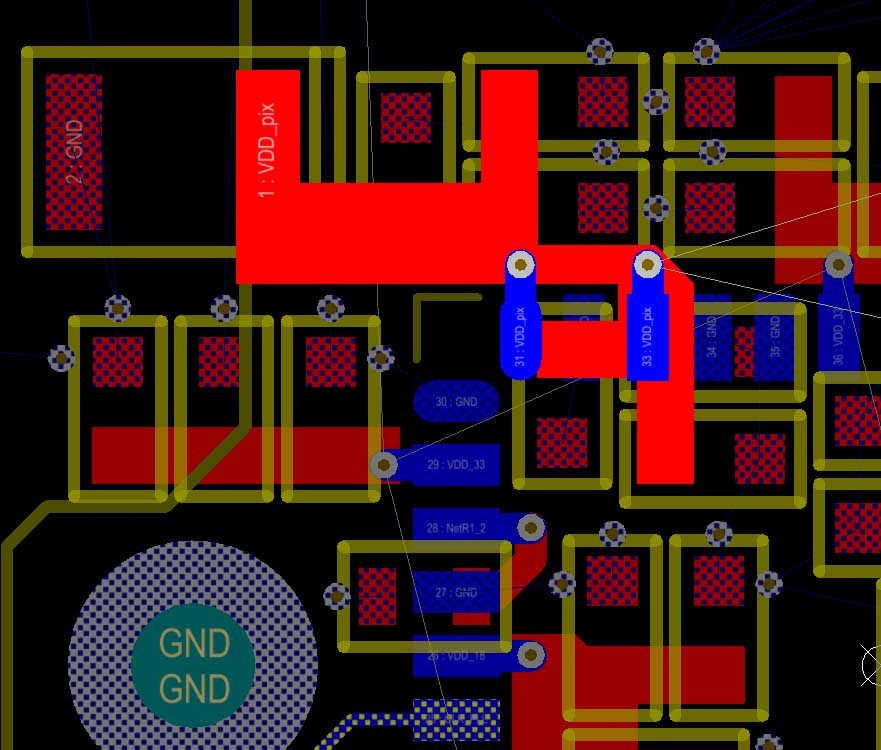
It is not clear from the pictures what are values of the capacitors and which components are decoupling capacitor. I can only guess and if I am guessing right, normally I do not place capacitors this way e.g. having two capacitors, where one is "behind" the other one and they are both connected to a VIA in front of the first capacitor. E.g. you could maybe place them under the blue pins (talking about the first picture)?
PS: To answer your VIA question, if possible, I use at least one through hole VIA per pin, if maximum current requires it, I use more VIAs. Often I also make a polygon plane which connects more VIAs and capacitors together, no problem.
I hope this helps.
PS: To answer your VIA question, if possible, I use at least one through hole VIA per pin, if maximum current requires it, I use more VIAs. Often I also make a polygon plane which connects more VIAs and capacitors together, no problem.
I hope this helps.
atantot , 09-21-2017, 12:54 PM
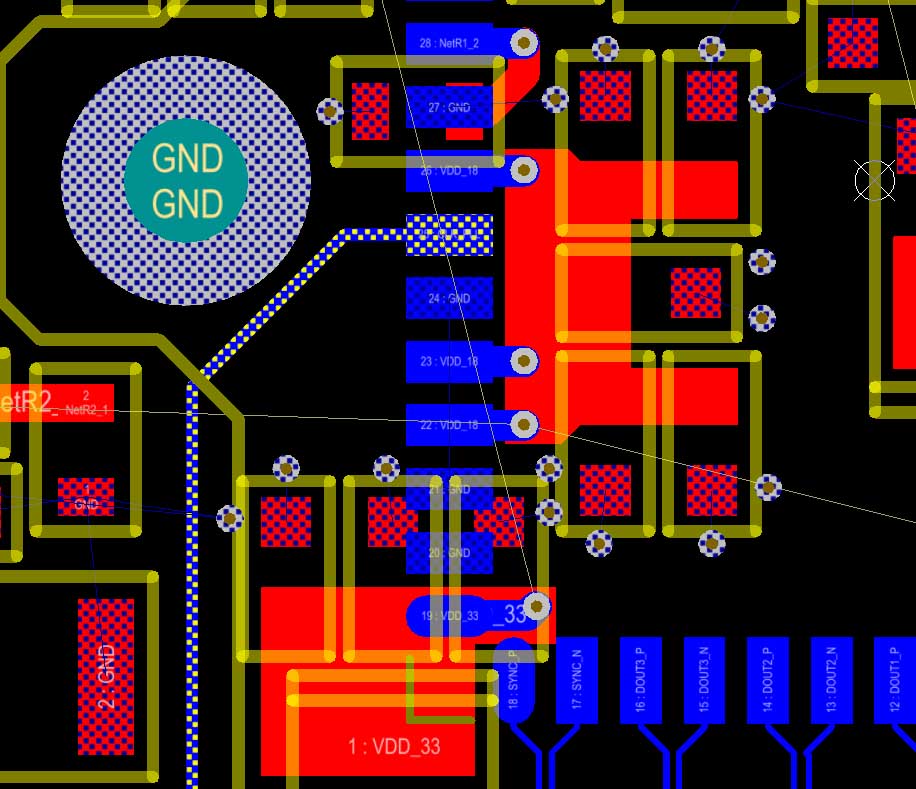
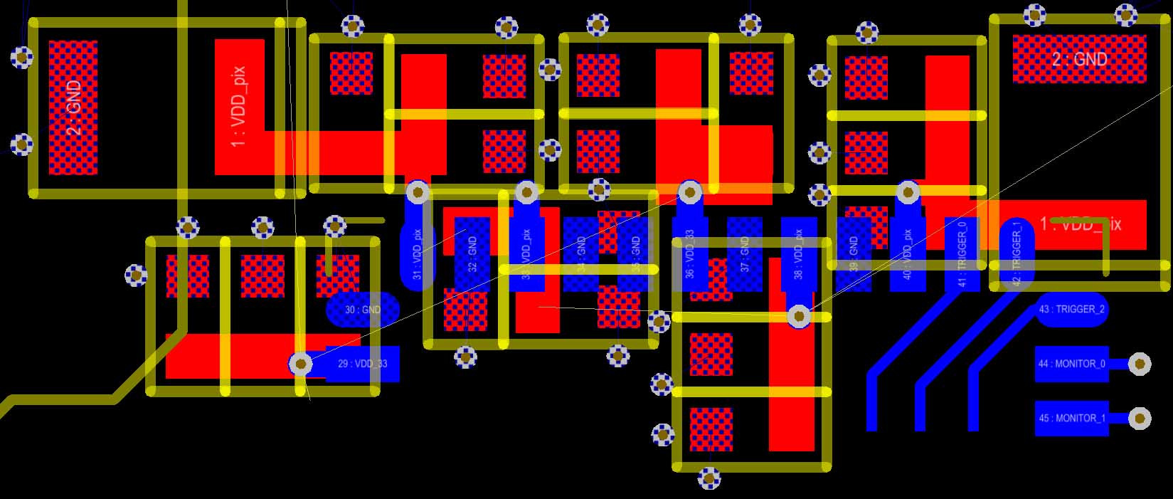
The pictures were not very clear, sorry. I added another one.You can only see the image sensor (the blue pads) and the decoupling capacitors (red pads). (I artificially added black rectangles to hide some components and pads that was not interesting now). All the visible components on the top are decouping capacitors. On the eval board, they have for each power pins at least 3 caps: 100 nF, 1 uF and 4.7 uF. There are also two larger caps of 100 uF.
So, the power pins:
* pin 29 - VDD_33 (gnd pin 30): 100 nF + 1 uF + 4.7 uF
* pin 31 - VDD_pix (gnd pin 32): 100 uF + 100 nF + 1 uF + 4.7 uF
* pin 33 - VDD_pix (gnd pin 34): 100 nF + 1 uF + 4.7 uF
* pin 36 - VDD_33 (gnd pin 35): 100 nF + 1 uF + 4.7 uF
* pin 38 - VDD_pix (gnd pin 37): 100 nF + 1 uF + 4.7 uF
* pin 40 - VDD_pix (gnd pin 39): 100 uF + 100 nF + 1 uF + 4.7 uF
I tried to follow your advice and to place the pins closer to the blue pins. Is it actually possible not to have a cap "behind" the other when there are that many caps per power pin? I'm quite surprised how many caps they use on the eval board, but I'm really not experienced enough to actually judge how relevant they are.
Does that make sense to place that many VIAs on the ground side of the capacitance, or one would be enough?
robertferanec , 09-27-2017, 08:35 AM
You are saying, "I'm quite surprised how many caps they use on the eval board" ... so, I would have a look how they placed the capacitors there. Maybe that could help you.
Paul van Avesaath , 10-02-2017, 03:32 AM
as far as the amount of caps, since it is an image sensor it can be because they really want to make sure there is no interferance from the power supply voltages. it all depends on how clean your power supply is. in general place the smalles caps as close to the pin and the more " bulk capacitance" like the 4.7uF and 100uf can be a bit further off. but if you can see it on the reference design it can give you a good indication of how it could go. with regards to the via count. again it helps if you know how much power is used. that will detemine the amount of via's needed. in general... more is better!! if you want to calculate how much power can go through your via you can use the saturn pcb toolkit (free to download) and put inyour via dimensions and see what you need and how many..
good luck!
good luck!
atantot , 11-10-2017, 08:27 AM
As Robert and Paul suggested, I finally used a design as close as possible to the reference design. For the exact layout and the number of vias, I did follow the basic rules but I convinced myself that I was probably overthinking it...
Anyway, the design has now been fully tested and it works as expected. Please see the attached picture ! Thank you for your support
I guess the next question is: "would that work with less decoupling capacitors?".
PS: Thank you for the saturn pcb toolkit
Anyway, the design has now been fully tested and it works as expected. Please see the attached picture ! Thank you for your support
I guess the next question is: "would that work with less decoupling capacitors?".
PS: Thank you for the saturn pcb toolkit

robertferanec , 11-10-2017, 07:35 PM
I love your board! Please, could we share it on our FEDEVEL Academy instagram and facebook?
PS: You can try unfit some capacitors, only the question is, if it is worth it - depends how much you could save when you unfit some capacitors and how sensitive the board price is comparing to stability and reliability.
PS: You can try unfit some capacitors, only the question is, if it is worth it - depends how much you could save when you unfit some capacitors and how sensitive the board price is comparing to stability and reliability.
atantot , 11-10-2017, 09:17 PM
You can share it but I'm really not so proud of it... Even tough that's my first 6-layer board, it is extremely close to the ref design... I just removed some components, changed board dimensions, connector, lens holder for the camera, etc. I'm happier about the micro-coax (awg40) lvds cable (custom made in China) for this board.
Thank you for the piece of advice The only reason that I would remove some capacitors is that I would like to reduce the board size at the next iteration... I'm planning to find smaller packages for the power supply and for some capacitors. Since this board was my first serious assembly and use of a reflow oven, I feel now more comfortable to go on smaller components !
Thank you for the piece of advice
The only reason that I would remove some capacitors is that I would like to reduce the board size at the next iteration... I'm planning to find smaller packages for the power supply and for some capacitors. Since this board was my first serious assembly and use of a reflow oven, I feel now more comfortable to go on smaller components !robertferanec , 11-11-2017, 09:26 AM
You can share it but I'm really not so proud of it... Even tough that's my first 6-layer board, it is extremely close to the ref design... I just removed some components, changed board dimensions, connector, lens holder for the camera, etc. I'm happier about the micro-coax (awg40) lvds cable (custom made in China) for this board.
I feel now more comfortable to go on smaller components !
atantot , 11-12-2017, 08:41 AM
Thank you! Please go ahead if you want to share it!
Your Youtube videos and your course on switching power supplies really helped me out for the two boards I designed (the green boards in the attached pictures). So the next steps is to go smaller as I said, but also to merge the two large boards into a single one (Zynq and DDR3). I'm waiting to have enough time and money to follow your advanced courses
Your Youtube videos and your course on switching power supplies really helped me out for the two boards I designed (the green boards in the attached pictures). So the next steps is to go smaller as I said, but also to merge the two large boards into a single one (Zynq and DDR3). I'm waiting to have enough time and money to follow your advanced courses


Use our interactive Discord forum to reply or ask new questions.