Unable to see net names to draw polygons
Art , 02-23-2017, 06:07 PM
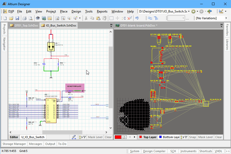
I am unable to to see the nets being marked 5V, 3V, GND and so on in the PCB layout while I have it all marked up in the schematic. Please take a look at my project and advice
mairomaster , 02-24-2017, 01:45 AM
If I understood correctly, you need to use cross probing. Enable cross select mode from Tools - Cross Select Mode. After that you can use the cross probe tool (Tools - Cross Probe) to click on nets/components which you want to highlight in both schematics and PCB at the same time. It is useful to split the work area in two so that you can see both schematics and PCB at the same time. You can also select a bunch of components and they will be highlighted in the PCB:
robertferanec , 02-24-2017, 09:31 AM
@Art, please read the article recommended by @mairomaster, and also have a look here, this may help you: Altium – Component Placement & Probing (The New & Old Way)
Use our interactive Discord forum to reply or ask new questions.